SECTION 1: Advanced Semiconductor Engineering
- Semiconductor Process
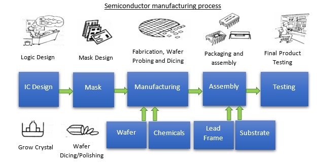
- Wafer Fab Processing and development
- Basic Processing Steps
- Starting Material – Bulk Silicon Process
- Wafer Specifications and Defects
- Silicon on Insulator Process
- Epitaxial Growth Process
- Deposition
- Oxidation
- Diffusion
- Ion Implantation
- Dry Etching Processes
- Wet Etching Processes
- Chemical Mechanical Planarization
- Lithography – Introduction
- Lithography – Resolution
- Lithography – Resists
- Lithography – Subwavelength Issues
- Lithography – Future
- LOCOS and STI
- Salicide and BEOL
- The Evolution of Each Processing Step
- Discussion over the trend of semiconductor
- Evolution of semiconductor and wafer fab
- Current Issues in Wafer Fab Processing
- Brainstorming on the understanding of Wafer Fab challenge
- The modern electronic circuits have now been evolved into ultra-large-scaled integrated (ULSI) circuits with extremely high performances. Discuss about the complicated issue facing Wafer Fab processing and yield development.
- Combining with artificial intelligent circuits and sensors, high intelligent robots may even perform better than human beings in some jobs such as elderly care and microsurgery. To realize such high intelligent systems, new integrated circuits with much higher performance and less power consumption are indispensable. What are those new challenges in the wafer fab process and how can those affect final product parameter shift, and the quality of the product engineering
- Current Issues in Assembly and Packaging
- Assembly and Packaging Processes Introduction
- Package Types
- Package Design Principles
- Leadframes
- Wire Bonding
- Lead Finish and Trim – Solder Ball Attach
- Die Attach
- Transfer Molding
- Packaging Business Issues
- Current Issues in Wafer Probing and Final Testing
- Automatic Testing Overview
- Wafer Probing
- Prober development
- Planarization issue
- Probe card development and issue
- Boundary Scan Overview
- Defect Classes
- Tester and instruments
- Test Process Basics
- Timing Tests in Production
- Class and QA Test limit
- Intermittent Testing
SECTION 2: Product Engineering Building Block
- The Advanced Product Engineering Development
- Circuit Evolution from 1960 to Beyond 2000
- New Product Introduction
- Product Development Cycle
- Product Datasheet and Parameters
- Manufacturing Challenges for 45nm and below
- Product Engineering and the yield performance with downsizing
SECTION 3: Product Guardbanding
- NPI Proof of Concept, Prototype design and validation
- Process Parameter shift
- Guard banding concept and practicality
- Determination of the Optimal Guardbanding
- Acceptable Risk Decision in the Declaration of Conformity
- Thermal Guardbanding
- Reliability Concern Shift due to Chip Design vs Guardbanding theory
SECTION 4: Operational Life Test (OLT)
- Bathtub Theory and Challenges in Modern World
- Understanding Product Engineering perspective
- Understanding of Economic perspective
- Process improvement methodology
- Infant Mortality (Early Life Failure)
- Failure rate goes down quickly from high to low as most failures are design / process flaws rooted
- Discussion and process engineering method
- Useful Life
- Failure rate remains low and steady with random causes to failure (e.g., EOS failure)
- Discussion and process engineering method
- Product Engineering viewpoint
- Wear Out.
- Failure rate rises sharply due to product aging
- Cost Saving Method
- Different test methods applicable for different failures.
- Temp Cycle
- Temp Cycle Pro and Cons
- Temp Cycle Guardbanding
- Reliability Guardbanding
SECTION 5: Reliability
- Concept of Semiconductor Device Reliability
- Dependencies of Failure Rate Function
- Early Failures
- Random Failures
- Wear Out Failures
- Screening and Quality
- Characteristics of Semiconductor Reliability
- Probability Distribution Used for Reliability Analysis
- Reliability Criteria
- Early Failure Period CriteriaRandom Failure Period Criteria
SECTION 6: Reliability Testing
- BI(Burn-in) / ELFR(Early Life Failure Rate)
- For assessing failure rate in the Early Failure section
- Reducing Early Life Failure Rate via the Burn-in approach.
- Theory on DPPM (Defect Parts Per-Million)
- HTOL(High Temperature Operating Life)
- Assessing the span of operating life
- Theory on FIT or MTTF
- HTGB (High Temperature Gate Bias)
- HTRG (High Temperature Reverse Bias)
- BLT (Bias Life Test)
- IOL (Intermittent Operation Life).
SECTION 7: Statistic Theory
- Six Sigma Theory
- Six Sigma and PPM
- Yield and Six Sigma
- CPK
- CPK and Yield
- Product Engineering vs CPK and Yield and PPM
SECTION 8: Failure Mechanism
- Failure Mechanisms Related to the Wafer Process
- Time Dependent Dielectric Breakdown
- Hot Carrier
- NBTI (Negative Bias Temperature Instability)
- Electromigration
- Stress Migration
- Soft Error
- Reliability of Non-Volatile Memory
- Failure Mechanisms Related to the Assembly Process
- Wire Bonding Reliability (Au-Al Joint Reliability)
- Ag Ion Migration
- Al Sliding
- Mechanism of Filler-Induced Failure
- Whiskers
- Moisture Resistance of Resin Mold Semiconductor Devices
- Failure Mechanisms Related to the Mounting Process and During Practical Use
- Cracks of the Surface-Mounted Packages in Reflow or Flow Soldering
- Failure Mechanisms Related to Electrostatic Breakdown and Electrical Overstress Breakdown, Latchup, and Power Devices
- Electrostatic Breakdown and Electrical Overstress Breakdown
- Latchup
- Power MOS FET Damage
SECTION 9: Test Methodology diagnose into Product Engineering
- Analog and Digital Test
- ATE
- Instrumentation Gauardbanding
- Class and QA Testing
- Shift of parameter over process and time
- Specific understanding into Advanced Theory for Final Test
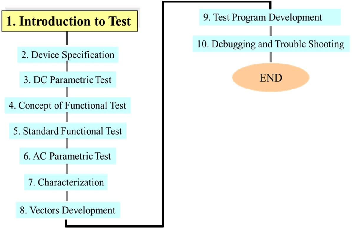
- Basic terms used and The purpose of testing in 21st century
- Components of test system
- Pin electronics card and PMU
- Basic rules for Test Engineering integrated into Product Engineering
- Characterization
- Common characterization parameters
- Methods and tools used to perform characterization
- Issues concerning device characterization
- PM and TPM
SECTION 10: Test Engineering Test
- Understanding of Basic Test Engineering and its importance to Product Development
- Test and Exams for Testing theory
- The roles and responsibility of product engineers
- The relationship and how to work with test, assmebly, packaging and wafer probe department for the efficiency of proudct engineering yielding.
Trainer : Lee Soong Yee (Malaysian)
Experience:
- Chief of Engineers and Engineering Manager for New Product Introduction and IC Product Testing department, Motorola USA(8 Years)
- Engineering Manager and Head for R&D department, chief engineering trainer, IRIS Corporation, Malaysia(3 years)
- Senior Engineer, National Semiconductor Corporation, USA(8 Years)
- External post graduate degree supervisor and examiners for master cum PhD degree, Malaysia Universities and oversea universities Malaysia campus.
- Content writer, author and course content developer for technical and engineering training courses, wrote for training company in Malaysia, Singapore, Indonesia, Taiwan and Vietnam
- Former City councillor, Petaling Jaya Municipal, Malaysia
- Consultant and engineering trainer, for few training companies in Malaysia, Singapore and Brunei (Currently)
- CEO, CatEagle Engineering Sdn Bhd(Currently)
- Principal, CatEagle Translation & Training (Currently) – Approved interpreter for United Nations, International Arbitration Center, High Court and Inter-Government meeting )
Specialty:
- Conducted technical and engineering trainer to engineers, technical staff, MNC and university lecturers – 15 years
- Conducted leadership and development training to corporate executives, managers and management team – 8 years
- Iris corporation chief trainer (For all technical training)
- Motorola University trainer (For technical and engineering training)
- Simultaneous interpretation, language translation, conducted over 1000 hours of simultaneous and consecutive interpretation and 12,000 pages of translation.
- Provide multi discipline of engineering training, technical training, management training, – approximately over 1000 training hours of engineering system, manufacturing training, to MNC staff, CEO, Managers, university lecturers, associate professors, professors, engineers, executives, engineering manager and technicians.
- Engineering management, engineering consultancy and factory operation.
Society Activities:
- Methodist church (Ampang parish) chairman, and lay leader (means head of the church executive committee).
- Ampang Chinese Methodist Church local lay preacher
- Active in society activities and volunteer organization and NGO
- Two chairman for social agency
- Currently 6 positions as committee member for social organization